To all my loved ones, cheers ♥
Theme adapted from orderedlist
Modern Storage Hierarchy: From NAND SSD to 3D XPoint (Optane) PM
01 Jan 2021 - Guanzhou Hu
As minimization and cell density of traditional 2D NAND SSDs reach a manufacturing bottleneck, 3D NAND SSDs come on the market. They push block capacity a little bit forward, but suffer from severer write amplification and are more expensive, thus are not a perfect solution. Intel 3D XPoint (official brand name as Optane), a hybrid design sitting in-between DRAM and NAND flash storage, adds a new possibility in the storage hierarchy.
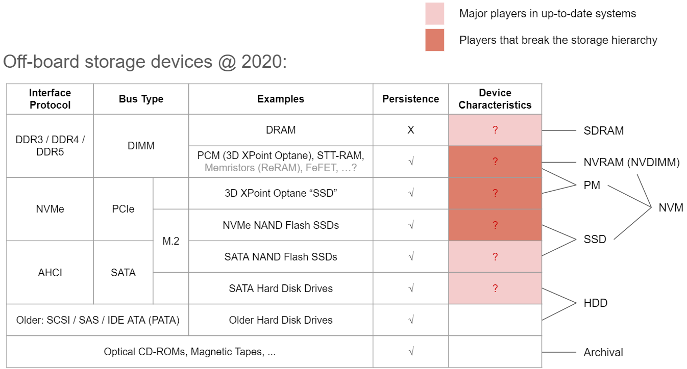
Non-Volatile Memory (NVM) & The Modern Storage “Hierarchy”
The name non-volatile memory (NVM) may refer to different ranges of things under different contexts.
- Broadly speaking, NVM refers to all kinds of persistent storage that maintains information “even after having been power cycled”1;
- Narrowly speaking, NVM refers to semiconductor memory chips without mechanical structures, including flash memory (such as flash chips, SSD) and ROM;
- Recently, NVM may refer to memory chips that are both persistent and byte-addressable. One example is Intel 3D XPoint. This category is often referred to as persistent memory (PM), NVRAM, or NVDIMM.
In the context of storage systems research, when people say NVM, they often mean the third definition. Designing storage policies and building file systems for novel NVM hardware is currently a hot topic. The storage “hierarchy” has now become an entangled pyramid where different types of devices have complex & overlapping performance characteristics. To be strict, it is not a hierarchy any more.
2D NAND Flash Architecture
A traditional 2D NAND SDD consists of a bunch of NAND flash packages together with an on-device controller and an on-device DRAM cache.
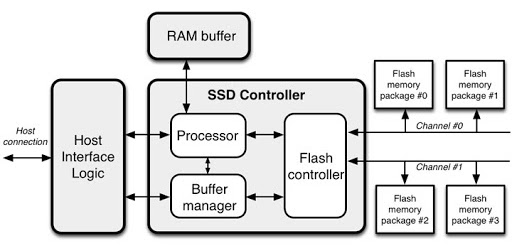
Figure by Emmanuel.
A NAND flash package is a set of planar NAND blocks, each having the following architecture:
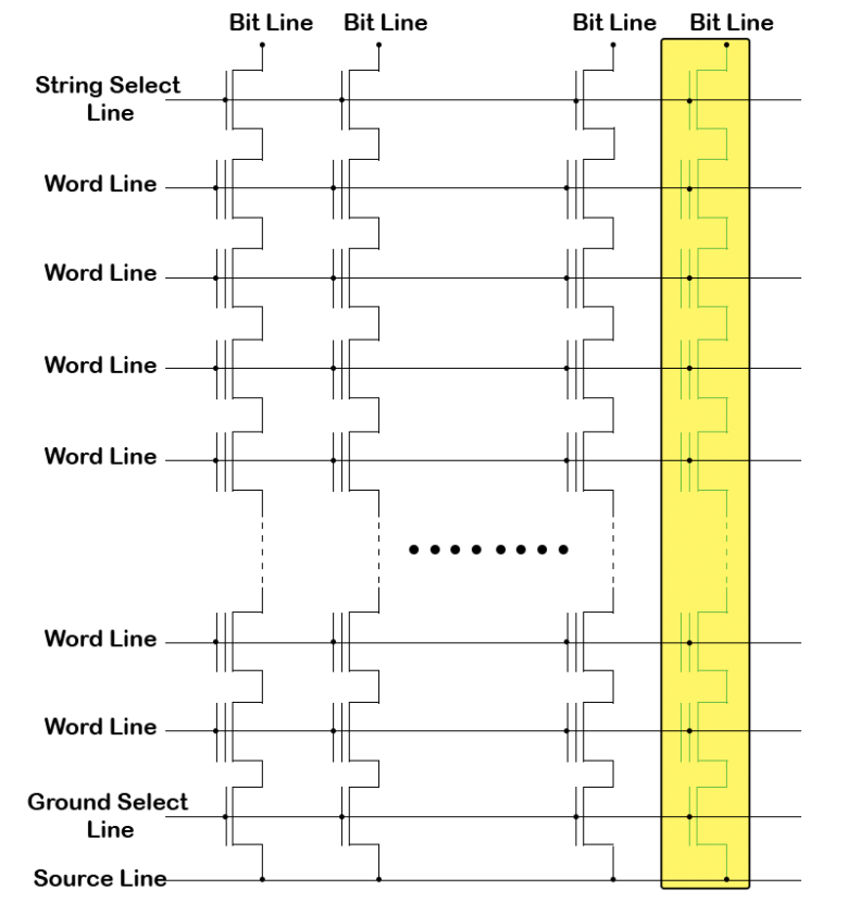
Figure from this post.
Every intersection of a word line and a bit line is a cell. A word line controls a page (for example 4KB), and a bit line connects a string. A block can contain, for example, 128 pages. Initially, all cells are not charged and represents a “1”. When a cell is broken-down and charged, it represents a “0”.
The smallest unit of reading is a page. Reading a page follows the procedure:
- Set selected page’s control gates to 0V, allowing cells to naturally leak voltage;
- Pre-charge all the bit lines, then wait for the cells to naturally leak voltage;
- Cells charged with negative charge will have weaker leak current:
- \(\rightarrow\) will have higher voltage after a short period of time
- \(\rightarrow V_{ref} < V_{bit}\) after a short period of time
- \(\rightarrow\) reads logical “0”
- Accordingly, uncharged cells will have \(V_{ref} > V_{bit}\), thus reads logical “1”.
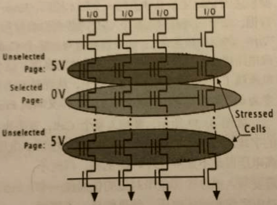
The smallest unit of writing is a block, unless writing on continuous free pages at the end of block. Writing a block follows the procedure:
- Leak all the negative charges to erase the whole block to “1”s;
- For each page in order, select its page line, giving high voltage at control gates:
- for cells that need to written “0”, ground their bit lines
- so that the cell will be broken-down and charged (i.e., written “0”).
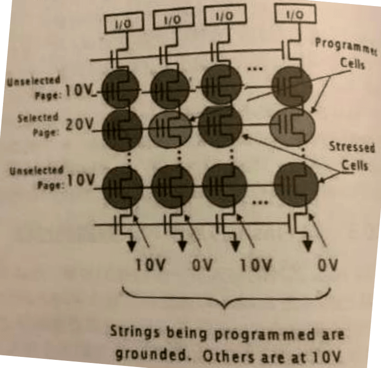
Figures from the book《大话存储》Chapter 3, by 张冬, 2015.
The fact that NAND SSDs must erase a whole block before updating it is a significant drawback. NAND SSD controllers must equip themselves with the following two functionalities in order to be useful and robust2:
- Wear leveling: on updates, we cannot simply read out the whole block into controller, erase the whole block, and then write back the updated block, because that will involve too many breaking-downs of cells. A cell has very limited life of break-downs and cannot afford one re-charge per update to its residing block. Thus, SSDs do redirecting on writes (RoW) - append the updated content somewhere cold and redirect subsequent reads to that new location, in order to make all blocks evenly wore. However, what if the new block is not empty and contains data? That data needs to be collected and moved somewhere else, resulting in extras writes.
- Garbage collection: if some pages of a block is invalidated (say, the file occupying them is deleted, or redirected) while other pages are still valid, we cannot simply treat the invalidated pages as free space and do new writes to them. Thus, those pages are logically freed but cannot physically serve as free space. They become “garbage”. SSDs do periodic background garbage collection, gather valid pages from several garbaged blocks, combine them and write them to a new block, and then erase (free) the garbaged blocks to clean out free space. These are extra writes as well.
When a write arrives at the drive, wear leveling and garbage collection cause a lot more data (than the size of the original write) to be actually moved and written. This is the notorious effect called write amplification. Typical write-amplification factor (WAF) on NAND SSDs ranges from 5x - 20x. This makes NAND SSDs perform dramatically poor at workloads involving many random writes.
Well…, is it actually? Maybe we should avoid using terms like “random writes” as they are designed for HDDs! Check out this paper.
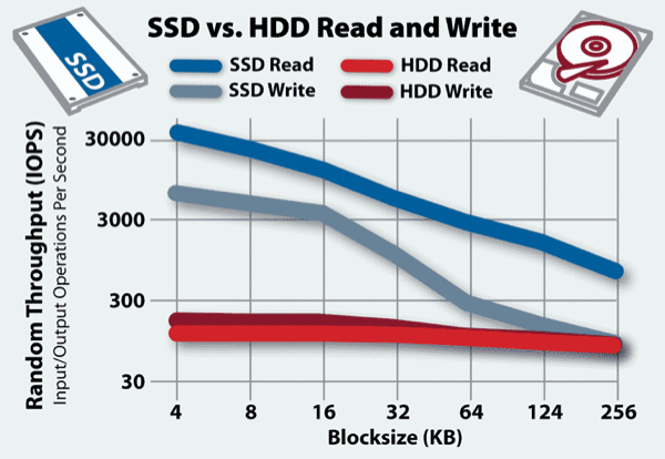
Figure from this post.
NOR flash has independent bit lines and is byte-addressable, but is much larger in size and not very practical.
3D NAND Flash Design
As the manufacturing of 2D NAND SSDs reaches its limit, people start to jump out of pure planar design and explore a third dimension.
- From SLC to MLC, TLC, & QLC: instead of single-level cells that can only represent “0”/”1”, we further divide the voltage level and thus every cell can represent 4 levels (2 bits, multi-level cell, MLC), 8 levels (3 bits, triple-level cell, TLC), or even 16 levels (4 bits, quad-level cell, QLC). The downside is that the cells become less robust and have significantly shorter life cycle.
- V-NAND flash: physically vertically stack the planar flash blocks.
These 3D designs give larger capacity to each flash block. However, that also makes write-amplification worse. Manufacturing cost also becomes a lot higher. It is believed that 3D NAND SSDs will not fully replace 2D NAND SSDs3.
3D XPoint (Optane) Technology
Intel proposes a new design of solid-state storage hardware called 3D XPoint on 2015 and release it to market under the brand name Optane on 20174. Through several years of development, this design yields the fastest SSDs available on market, and is often thought of as the next-generation state-of-the-art persistent storage hardware.
This technology is a successful example of phase-change memory (PCM) hardware - one of the most promising directions towards building non-volatile RAM. As the name 3D XPoint describes, memory cells are put at cross points of a 3D grid. It truly makes persistent storage “3-dimensional”.
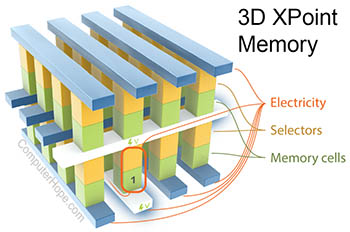
The most appealing property of 3D XPoint is that it is persistent meanwhile byte-addressable. This means that it sits in between current NAND SSDs and DRAM volatile memory on the storage hierarchy (has smaller capacity than NAND flash but comparable capacity than DRAMs; has lower speed than DRAMs but faster speed than NAND flash; and it is durable). It can be treated as either, depending on the workload.
The name sometimes refers to Optane DIMM / Optane SSDs specifically. Optane DIMMs connect to the memory bus and is directly controlled by the processor cache system. Details about its internals can be found in this recent paper 5. Optane SSD products use the same PCM media technology, but expose a traditional NVMe SSD interface.
Optane DIMM Performance & Consistency
As this paper pointed out, the current state of Optane DIMM exposes some interesting performance characteristics that lie in the middle of SSDs and DRAM:
- Latency performance approaches DRAM, but has larger variation;
- Though the whole device appears to be byte-addressable, small random accesses matter - they will bring down performance due to the 256B actual media granularity;
- DRAM is serial, SSDs have high internal parallelism across packages, and Optane DIMM sits in between - it has limited degree of internal parallelism and hence degraded performance under high concurrency;
- Ordering of temporal accesses to the same memory address is important due to consistency issues.
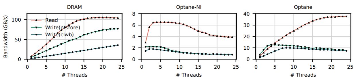
Figure from the Yang, et al. paper, Figure 4.
Whenever there is caching across volatile/non-volatile media, there are consistency issues. Imagine two user requests: ① appending a new element to a data structure, followed by ② incrementing a counter in data structure header. It is possible that both requests hit in cache and, at some time later, the update ② gets evicted earlier than ①. If the system crashes at this point, the state is left inconsistent. After recovery, the user may check the header counter and may believe that the newly appended index contains valid data, while it is not - that data has not yet been persisted on storage media - so the user may read out some garbage.
For traditional disk-based FS, the volatile cache is the in-memory buffer cache, and the persistent storage is the disk drive. We do journaling with fsync()’s to maintain the ordering of requests. For NVDIMM, the volatile cache is the CPU cache, and the persistent storage is the NVDIMM chip on memory bus. NVM systems do journaling with mfence & clflush instructions to maintain such ordering. Some ad-hoc data structures (e.g., B-trees) running over NVM may directly deploy their own ordering constraints w/o the help of a system layer.
Designing storage systems and building file systems for NVM is currently a very hot topic in storage systems research. This is a good example of how an evolution in hardware leads system software research. I believe this technology adds a new possibility in building storage systems and will make future storage systems design more flexible and more efficient.
References
Comments welcome! 😉